by Bruce DeChillo, Product Manager, Aries Electronics, Bristol, PA USA
Cellular phones, pagers and PCSs are at the forefront of wireless communication. Manufacturers of the components used in these applications must carefully test their devices, making a properly configured high-performance test socket a key part of the testing equation.
“High-performance” means two things in terms of test sockets: achievement of a substantial number of device insertions before the socket needs replacing; and the display of superb electrical performance. As the frequencies of devices used in wireless applications increase, test sockets must be able to perform at higher frequency levels.
There are two key areas of concern when evaluating various test socket: 1) reliability, and 2) performance.
Reliability
A socket’s reliability is crucial to help lower the cost for each device tested. Ideally, a socket should require no repair, and operate reliably during its full life cycle. In reality, it will need cleaning, repair or replacement. Cleaning can require a complete breakdown of the test board. Repairing a socket almost always requires test board breakdown, followed by another setup. Socket adjustments, although performed infrequently, use up valuable test time. As a result, throughput is lowered and cost-per-device tested is increased.
Temperature can affect socket life and reliability. Each device must be tested under the same conditions at which it will be used, and test temperature extremes can range from -55°C to +150°C. Naturally, sockets that can withstand these temperatures through hundreds of thousands of cycles are more expensive than conventional test or burn-in sockets, but they will pay for themselves through long service life.
Thermal considerations involve continuous service temperature and Coefficient of Thermal Expansion (CTE). Different materials expand at different rates under the same temperature conditions, so the housing material must be flexible enough to accommodate the se variations, and tough enough to withstand them.
Occasionally, a socket contact, or the socket itself, must be replaced. This can result from simple wear-and-tear, or from using a socket that’s inadequate for the purpose. In both cases, the situation incurs the downtime cost and time needed to effect the repair, and cost of replacement parts.
Performance
Performance is the second major concern for production of wireless IC’s. The ideal test socket should be electrically “transparent;” that is, its presence will have no effect on the test results. This characteristic can be achieved with a low self-inductance and capacitance between contacts, and the contact’s ability to maintain controlled impedance.
A socket’s high-frequency capability is inversely proportional to its contact inductance. High lead inductance values can lead to unwanted oscillations and signal degradation. That’s why package engineers concentrate on developing packages with low lead inductance.
Inductance and capacitance influence the overall impedance value of the socket contacts. Therefore, the test socket’s contact impedance should closely match that of the device package. Impedance mismatches can lead to signal reflections, which can cause signal loss and oscillations.
Impedance is a complex term that defines the resistive and reactive elements of an electrical signal medium, whether it’s a wire or printed circuit board (PCB) microstrip trace. The resistive element is determined by the wire’s resistance (Ohms, Ωs) and the reactive element is determined by the inductance (Henry, H) and capacitance (Farad, F) of the PCB microstrip trace. As an electrical signal travels through a trace, its fundamental characteristics change as the impedance changes. And as the signal’s frequency increases, so does its reaction to the change in impedance.
Although it’s relatively easy for board designers to match lead impedances, it’s often difficult for socket manufacturers to do likewise. Most sockets simply do not have any means of impedance control.
Mutual inductance and capacitance characteristics pose other problems. As a signal’s frequency increases, so does its electromagnetic field. If the socket’s design and materials of construction contribute to coupling characteristics, then unwanted electrical “cross-talk” between these fields will promote the development of oscillations, reduce gain level and increase signal degradation, with a subsequent detrimental effect on performance.
THEORY AND REALITY
How does this translate into actual practice? Let’s examine two key components of a high-performance test socket – the housing and the contacts.
Polyetherimide is a typical housing material. It is a thermoplastic that displays excellent mechanical, thermal, and electrical properties. In production settings, automated device handlers are widely used. It’s important that the housing’s mechanical specifications are close to those of the handler’s plunger mechanism (which is usually made of polyamideimide) because these two parts can come in contact with each insertion of an IC package. Flexural strength is also critical, because of the repeated cycle of pressure and release that occurs when the housing is used as a hard stop to eliminate damage to the device under test.
The continuous service temperature rating for polyetherimide is -60°C to +170°C that exceeds even the strict temperature testing range established for military applications. Ultem’s CTE is very low (3.1 x 10⁻⁵ in/in/°F), which helps maintain close dimensional stability of the housing for IC package alignment, and good coplanarity between the socket and test board.
The dielectric constant and dissipation factor of polyetherimide are 3.15 and 0.0015 respectively, at 1MHz – extremely respectable numbers for RF applications. These two specifications minimize the socket’s mutual conductance, thus reducing “cross-talk” and leakage currents at high frequencies.
CONTACTS
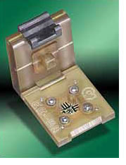
The heart of any test socket is its contacts, because they provide signal transmission paths between the device and the test board. Proper signal transmission depends upon proper contact design and implementation.
The Microstrip™ contact (patent owned by Aries Electronics) provides many of the characteristics required by high-performance testing. It provides minimal signal loss in high-bandpass applications, and delivers long cycle life (over 500,000 cycles) in automated handler testing. Additionally, it provides a virtually transparent connection between the device-under-test and the printed circuit board.
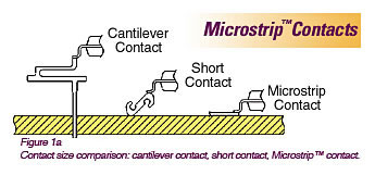 During test, the Microstrip™ contacts lie flat against the PCB microstrip, whereas short contacts and cantilever contacts introduce a significant signal path (2mm and 20mm, respectively), to the device-under-test. (See Figure 1a).
The Microstrip™ contact is made from 0.007″ [0.178mm] thick, Au-plated proprietary high-service life material, which was developed for its ease-of-processing and spring strength. Au plating provides low ohmic contact between the Au-plated test board trace and the Microstrip™ contact.
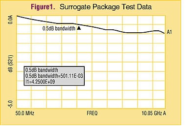
When the Microstrip™ contact lies flat against the PCM microstrip, it actually becomes part of the transmission line. The PCB microstrip and Microstrip™ contact can be designed with the same width, enabling designers to closely match the device’s lead impedance. The transition of the contact into the PCB microstrip leads to extremely low contact self-inductance and very low signal loss in high-frequency applications. (See Figure 1).
It requires less than 24 grams of contact force per contact with a 0.5mm lead pitch device (0.012″/0.304mm wide contacts), and features a built-in wiping action to remove surface debris, solder build-up and other possibly contaminated materials.
Manufacturers of components for wireless applications must test them thoroughly to ensure proper performance in the field. Careful selection of a high-performance test socket will contribute to accurate, repeatable test results, and to a lower cost per device tested.
CONCLUSION
As frequencies increase in wireless applications, greater attention must be given to socket selection. The best socket option will provide minimum inductance at maximum speed. The Microstrip™ contact is currently the optimum choice for meeting these stringent parameters.