CSP Test Socket for Optical Laser Failure Analysis w/Emission Microscopy*
Available with or without filters for UV, infrared and full spectrum applications, this optical test socket is ideal for testing an optical sensor type chip and for EMMI testing a standard chip using an infrared head sensor. The optical test socket line can accommodate many different optical window and lens materials, including glass, sapphire, and plastic depending on operational requirements. The standard optical grade window on the 23023 socket uses a high-quality quartz V077 glass with a 98% transmission rate from <260nm in the UV to >2000nm in the infrared.
FEATURES
- Aries unique universal socketing system allows the socket to be easily configured for any package, on any pitch (or multiple pitch) from 0.2mm or greater, in any configuration, with little or no tooling charge or extra lead-time.
- For Test & Burn-In of CSP, µBGA, Bump-Array, QFN, QFP, MLF, DFN, SSOP, TSSOP, TSOP, SOP, SOIC, LGA, LCC, PLCC, TO and any SMT package style made. Also can be compatible with PGA packaged devices.
- Quick and Easy Probe Replacement System: the complete set of probes can be removed and a new set (interposer) can be inserted quickly and easily. The old set can be returned to the factory for repair and sent back within one day.
- Socket lid nests device into socket for a reliable connection.
- ZIF style socket using Aries solderless, Au-plated pressure mount Spring-Probe.
- Special lid designs and/or materials can be quoted.
- Socket easily located, mounted & removed from PCB.
- Signal path during test only 0.077 [1.96].
- Available with Spring-Probes or Kapton Elastomer Interposer.
- 4-point crown insures “scrub” on solder oxides. Consult factory for other available probe styles.
- The Au over Ni-plated compression Spring-Probes leave very small witness marks on the bottom surface of the device solder balls.
CLEANING, HANDLING, MOUNTING
& PROBE REPLACEMENT INFO MOUNTING CONSIDERATIONS
- NOTE: Sockets must be handled with care when mounting or removing sockets to/from PCB
- TEST PCB MINIMUM DIAMETER "P"...
: 0.025 [0.64] (large probe 0.80mm pitch and larger)
: 0.015 [0.38] (small probe 0.50-0.79mm pitch)
: 0.012 [0.31] (small probe 0.40-0.49mm pitch)
: 0.009 [0.23] (small probe 0.30-0.39mm pitch)
: 0.004 [0.10] (small probe 0.20-0.29mm pitch) - TEST PCB DIA. SPRING-PROBE & KIP PAD PLATING: 30µ min. [0.75µ] Au per MIL-G-45204 over 30µ [0.75µ] min. Ni per SEA AMS-QQ-N-290. Pad must be the same height as top surface of PCB. Please refer to the Custom Socket Drawing supplied by Aries after receipt of your order for your specific application.
SPECIAL THERMAL REQUIREMENT WORKSHEET
GENERAL SPECIFICATIONS
|
|
TEST REPORTS
- Center Probe 0.4mm Socket Return Loss Test
- Center Probe 0.5mm BGA Socket Electrical Performance
- Center Probe 0.5mm Socket Return Loss Graph
- Center Probe BGA 0.8mm Socket Electrical Characterization
- Center Probe Contacts Decibel Frequency Graph
- Center Probe CSP Socket DC Cycling
- Center Probe CSP Socket DC Measurement
- Center Probe CSP Socket RF Cycling
- Center Probe CSP Socket RF Measurement
NOTICE | ORDERING INFORMATION | |||||||||||||||||||||||||||||||||||||||||
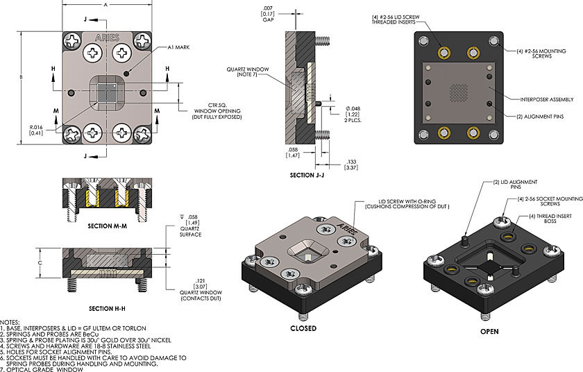
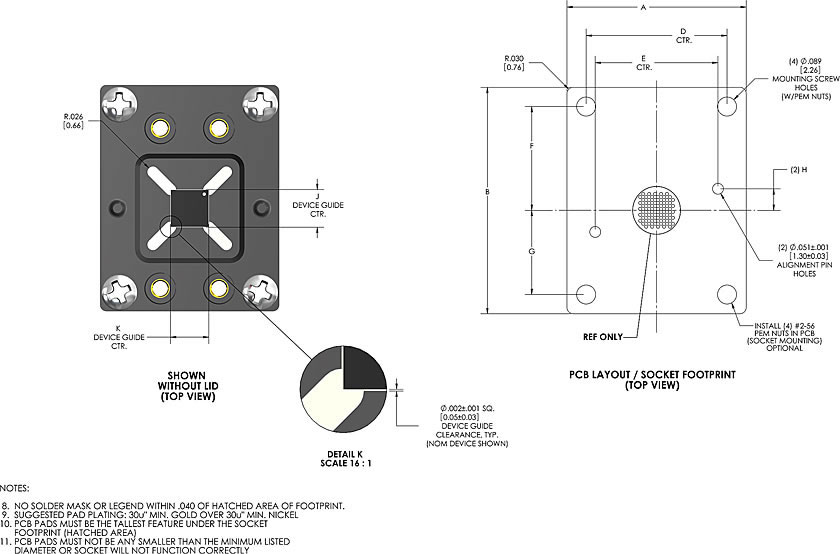
ALL DIMENSIONS: INCHES [MILLIMETERS] ALL TOLERANCES: ±0.005 [0.13] UNLESS OTHERWISE SPECIFIED CONSULT FACTORY for DIM. “A” - “K” CONSULT FACTORY FOR OTHER SIZES AND CONFIGURATIONS PRINTOUTS OF THIS DOCUMENT MAY BE OUT-OF-DATE AND SHOULD BE CONSIDERED UNCONTROLLED 
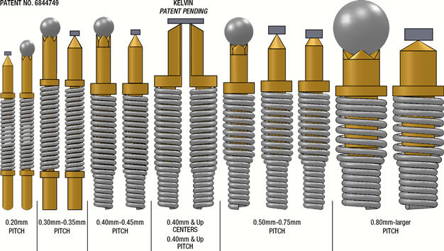
CUSTOMIZATION: In addition to the standard products shown on this page, Aries specializes in custom design and production. Special materials, platings, sizes, and configurations can be furnished, depending on quantity. NOTE: Aries reserves the right to change product specifications without notice. |
|
FULL-ARRAY SHOWN AS AN EXAMPLE; YOUR SPECIFIC DEVICE PATTERN/FOOTPRINT WILL BE SUPPLIED WHEN ORDERED. |
![]() |
Download Data
Sheet 23023, Rev 1.6 |