by Bruce DeChillo, Product Manager, Aries Electronics, Bristol, PA USA
INTRODUCTION
With rapid and constant advances in silicon technology, today’s IC packages are continually changing both inside and out. The inside of the package is holding more transistors per square millimeter. The outside of the package is constantly being trimmed and reconfigured to approach the size of the IC itself.
As a consequence, tremendous new challenges are placed on those who need to test these devices. Rise times, clock rates, and burst rates are becoming faster and shorter, while package pads and pitches are becoming smaller and tighter. Clock rates, in general-purpose computers, have increased a thousand-fold in the last 25 years. Data rates of 10GB/s are becoming the norm, instead of the exception in digital communication systems. In addition to higher response times, today’s test socket engineers and manufacturers must face a new challenge: higher frequencies. Wireless communications are edging to the far extremes of the microwave region (up to 35GHz).
TESTING THE IC PACKAGE
One of the key “backend” tests is the testing of the IC package itself. In this operation, the IC is tested after it has been sealed in its housing. Here the IC and packaging elements are thoroughly evaluated to determine if they will perform as required when soldered down to a PCB in their final application. Package testing is usually the final test before the devices are shipped to the customer, making it one of the most critical tests in the IC’s early life.
Perhaps the most critical element involved in final test is the test socket. Test sockets have been used for over 30 years in the characterization of IC packages. Most existing test sockets have limited frequency ranges – usually below 50MHz, with reliable performance specified of no more than 1GHz. Such designs cannot accommodate today’s microwave devices, much less tomorrow’s. Current socket designs that attempt to solve the problem tend to be large, have relatively short cycle times, require timely rework and, typically, have contacts with high self-inductance and mutual capacitance. This can cause unexpected degradation of the circuit’s overall performance.
When pulse edges are fast, or clock frequencies are high, some physical side effects, normally considered too small to affect design performance, become major factors. These characteristics change a socket from a passive signal carrier to an active element. The demand for clean signals at high-speeds has resulted in the need for custom-designed test sockets. Most attempts to meet this need have fallen short at the high-end radio frequencies. The few available sockets that do perform at high RF levels usually carry a hefty price tag.
NEW ADVANCES IN SOCKET TECHNOLOGY
In recent years, however, test sockets that can handle ultra high-frequencies have been developed. Suitable for manual test, handler and dynamic burn-in, this simple socket is surface-mounted and has a wide operating temperature range. Surface mounting is a must: a thru-hole socket introduces unpredictable impedance mismatches, stray capacitance and inductance.
The new RF socket line uses a compression fit between the socket contacts and the PC board microstrips, which ensures reliable performance with simple contact replacement. The contacts are secured to a contact block which is aligned with the microstrips by fixed alignment pins. The top-half of the socket is screwed down to the DUT (Device Under Test) board, compressing half the length of the contacts to the microstrips. To replace contacts, the top plate is simply unscrewed, the contact block removed, a new block aligned and the top plate screwed on. All of this is accomplished in less than five minutes.
An important element of the advanced RF test socket design is Aries patented Microstrip™ contact technology. Many high-frequency socket designs use the same contact design for all package leads. The subject contact design, in contrast, matches contact width to package lead width, which provides the largest surface area contact to all package leads. The contact also provides a wiping action. These features combine to provide extremely low contact resistance, with only 30 grams of force required for each contact.
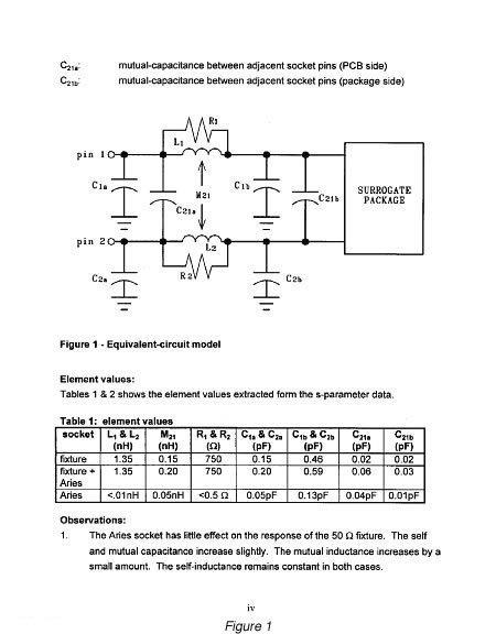
Of special interest to manufacturers of high-frequency devices, the wide blade construction provides outstanding performance well into the microwave region. The contact provides a practically transparent connection from DUT to PCB. With a standard lead length of 0.250″, the contact displays less than 0.01nH self-inductance in a 50Ω microstrip test environment. (see Figure 1)
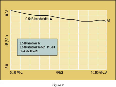
Testing was performed at Giga Test Labs, Cupertino, California, on a 20-pin SSOP Test Socket. The results demonstrated that these sockets can easily be used in microwave applications greater than 10GHz. (see Figure 2)
When the socket is fastened to the PCB, one-half of the socket contact lies directly on top of a microstrip which must be designed in the target PCB and should be the same length as one entire socket contact. The contact used in the above test measured 0.250″ (L) x 0.025″ (W) x 0.007″ (H). When the DUT leads are pushed against the socket contacts, the contacts flatten completely against the microstrip. The contact in effect become part of the microstrip, or transmission line, adding only 0.007″ in height. The height modification will increase impedance slightly, but by only a fraction of the standard impedance line designed at 50Ω.
Self-inductance is negligible because only 0.007″ is added to the device lead, or microstrip. Mutual capacitance is minimized, since the dielectric constant in the thermoplastic material, which holds the contacts in place, is around 3.0.
ACHIEVING TEST SOCKET RELIABILITY AND PERFORMANCE
Meeting high-frequency test needs is essential for device manufacturers developing ICs for wireless and related applications. To do so, the test socket must not only be capable of accommodating the high-frequency parameters, but must also deliver reliability and high-performance in doing so. For a test socket, high-performance means two things: 1) achieving a substantial number of device insertions before the socket needs replacing; and 2) the display of superb electrical performance.
RELIABILITY
A socket’s reliability is crucial if IC manufacturers are to achieve lowest overall cost for each device tested. Ideally, a socket should require no repair, operating with full reliability, during its entire life cycle. In reality, at some point in time, it will need cleaning, repair or replacement.
Cleaning may require a complete breakdown of the test board. Repairing a socket almost always requires test board breakdown, followed by another setup. Socket adjustments, although performed infrequently, use up valuable test time. As a result, throughput is lowered and cost-per-device tested is increased.
Temperature can affect both socket life and reliability. Each device must be tested under the same conditions at which it will be used, and test temperature extremes can range from -55°C to +150°C. Naturally, sockets that can withstand these temperatures through hundreds of thousands of cycles are more expensive than conventional test or burn-in sockets, but they will pay for themselves many times over through their vastly improved service life.
Thermal considerations involve continuous service temperature and Coefficient of Thermal Expansion (CTE). Different materials expand at different rates under the same temperature conditions, so the housing material must be flexible enough to accommodate these variations, and tough enough to withstand them.
Occasionally, a socket contact, or the socket itself, must be replaced. This can result from simple wear-and-tear, or from using a socket that’s inadequate for the purpose. In both cases, the situation incurs the downtime cost and time need to effect the repair, and cost-of-replacement parts.
PERFORMANCE
Performance remains a major concern in the production and application of high-frequency test sockets. The ideal test socket should be electrically “transparent;” that is, its presence has no effect on the test results. This characteristic can be achieved with low self-inductance and capacitance between contacts, and the contact’s ability to maintain controlled impedance.
A socket’s high-frequency capability is inversely proportional to its contact inductance. High lead inductance values can lead to unwanted oscillations and signal degradation. That’s why package engineers concentrate on developing packages with low lead inductance.
Inductance and capacitance both influence the overall impedance value of the socket contacts. Therefore, the test socket’s contact impedance should closely match that of the device package. Impedance mismatches can lead to signal reflections, which can cause signal loss and oscillations.
Impedance is a complex characteristic term that defines the resistive and reactive elements of an electrical signal medium, whether it’s a wire or printed circuit board (PCB) microstrip trace. The resistive element is determined by the wire’s resistance (Ohms, Ω) and the reactive element is determined by the inductance (Henry, H) and capacitance (Farad, F) of the PCB microstrip trace. As an electrical signal travels through a trace, its fundamental characteristics change as the impedance changes. And as the signal’s frequency increases, so does its reaction to the change in impedance.
Although it’s relatively easy for board designers to match lead impedances, it’s often difficult for socket manufacturers to do likewise. Most sockets simply do not have any means of impedance control.
Mutual inductance and capacitance characteristics pose other problems. As a signal’s frequency increases, so does its electromagnetic field. If the socket’s design and materials of construction contribute to coupling characteristics, then unwanted electrical “cross-talk” between these fields will promote the development of oscillations, reduce gain level and increase signal degradation, with a subsequent detrimental effect on performance.
CONCLUSION
Testing today’s high-frequency IC devices require a new breed of RF test sockets. These sockets need to meet performance and reliability criteria that are frequently as complex as the devices they are called on to help test.
Key elements in RF test sockets that can successfully meet today’s needs include: electrical response parameters that accommodate both the higher speed and higher frequencies of today’s RF devices; performance that is essentially transparent to the device in that it has no effect on the device or test; and reliability in that the socket minimizes the need for repair or replacement, thus lowering the overall cost of the tested device.
Fortunately, Aries newest breed of RF test sockets do include products that meet all these criteria.