by Bruce DeChillo, Product Manager, Aries Electronics, Bristol, PA USA
 Semiconductor design engineers have been under constant competitive pressure to provide more features and functions, all with lighter weights, smaller sizes, and lower costs.
In the early 1980s, these sometimes conflicting goals resulted in the birth of surface mount technology (SMT) but the universal adoption of SMT was neither fast nor painless, nor is it complete. Ten years after its introduction, only 50% of designs used SMT. The reason is that each reduction in package lead pitch required retooling throughout the industry. Package lead frame and assembly equipment had to be converted, as well as test handlers, sockets, surface mount equipment, not to mention assembly processes. Demand for smaller packages with more I/O’s resulted in new generations of dual-sided and QFP packages, all with lead pitches reduced to 1.0mm, then 0.8mm, then 0.65mm, then 0.5mm and below.
Trends in IC features and performance are evolving extremely rapidly. Clock rates in general-purpose computers are increasing by a factor of two every year, from 25MHz in 1989 to about 1GHz by the end of the decade. Data rates of 2GB/s or more are common in digital communication systems. Wireless communications are edging to the far extremes of the microwave region (from 1 to 35GHz).
These developments necessitate new methodologies for semiconductor testing. Socket designers are faced with a new challenge—frequency. Most manufacturers rely on increased functional testing for high-density assemblies, a trend that is sure to continue in wireless products where device probing can adversely affect circuit operation. High-performance testing of devices is the only method of assuring product reliability.
Most existing test sockets have limited frequency ranges, usually below 50MHz. The best specify reliable performance of no more than 1GHz. Such designs cannot accommodate today’s microwave devices, much less tomorrow’s. Current socket designs that attempt to solve the problem tend to be large, have relatively short cycle times, require timely rework and typically have contacts with high self-inductance and mutual capacitance. For high-frequency microwave devices, a poorly designed socket acts as a parasitic passive filter, which may cause unexpected degradation of the circuit performance as a whole.
When pulse edges are fast, or clock frequencies are high, some physical side effects, normally considered too small to affect design performance, become major factors. These characteristics change a socket from a passive signal carrier to an active element.
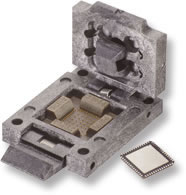
The growing demand for clean signals at high-speeds has resulted in a demand for custom-designed test sockets. Most attempts to fill this market gap have fallen short when it comes to high-end radio frequencies. The few available sockets that perform at high RF levels usually carry a price tag that matches the frequency. Aries’ RF test socket line handles ultra high-frequencies. Suitable for manual test, handler and dynamic burn-in, this simple socket is surface mounted and has wide operating temperature range. Surface mounting is a must: a thru-hole socket introduces unpredictable impedance mismatches, stray capacitance and inductance.
The socket uses a compression fit between the socket contacts and pc board Microstrips™, which ensures reliable high-performance with simple contact replacement. The contacts are secured to a contact block which is lined up with the Microstrips™ by fixed alignment pins. The top-half of the socket is screwed down to the DUT board, compressing half the length of the contacts to the Microstrips™. To replace contacts, the top plate is simply unscrewed, contact block removed, a new block aligned and the top plate screwed on, in less than five minutes.
An important element is the patented contact pins. Many high-frequency socket designs use the same contact design for all package leads. The Aries contact design, in contrast, matches contact width to package lead width, which provides the largest surface area contact for all package leads. The contact additionally provides a wiping action. These features provide extremely low contact resistance, with only 30 grams of force required for each contact.
The wide blade construction provides outstanding performance well into the microwave region. The contact provides a practically transparent connection from DUT to PCB. With a standard lead length of 0.250″, the contact displays less than 0.01nH self-inductance in a 50Ω Microstrip™ test environment. Testing was performed at Giga Test Labs, in Cupertino, California, on a 20-pin SSOP Test Socket. As the results show, these sockets can easily be used in microwave applications greater than 10GHz.
When the socket is fastened to the PCB, one-half of the socket contact lies directly on top of a Microstrip™ which must be designed in the target PCB and should be the same length as one entire socket contact. The contact used in the above test measures 0.25 0″ (L) x 0.025″ (W) x 0.007″ (H). When the DUT leads are pushed against the socket contacts, the contacts flatten completely against the Microstrip™. The contacts, in effect, become part of the Microstrip™, or transmission line, adding only 0.007″ in height. This height modification will increase impedance slightly, but by only a fraction of the standard impedance line designed at 50Ω.
The self-inductance is negligible because only 0.007″ is added to the device lead, or Microstrip™. Mutual capacitance is minimized, since the dielectric constant in the thermoplastic material which holds the contacts in place is 3.0.
The components of the socket perform well under thermal conditions. Increasing speed and decreasing geometry of modern semiconductors result in ever increasing power dissipation. Combine this with burn-in temperatures up to 150°C, and you have a very hostile environment, not only for the DUT, but for the socket holding the DUT as well. With 0.5mm lead pitches, material expansion cannot be tolerated.
The RF socket attacks the heat problem from two angles: 1) the thermoplastic material holding the contacts in place has excellent thermal stability; the CTE varies from 0.6 to 0.8-inch/inch/F, over a temperature range of 50°C to 170°C and the contacts are held in place by this material, prohibiting contact movement over this temperature range; 2) a large heat vent can be built into the overlapping tilt pad, which can also be used for probing purposes while the device is under test.